A medium power RF amplifier for lab use
Sometimes a small medium power broadband RF amplifier is handy for lab work if, for example, the output level available from a signal generator is not sufficient for a particular purpose. Applications include driving experimental circuits or testing the electromagnetic susceptibility of equipment or experimental setups. Of course, various connectorized amplifier modules are available from several manufacturers, and I already have a good collection of them, but in order to have some fun and to gain a bit of experience with modern LDMOS transistors I decided build a small broadband amplifier module myself.
The goal was to design a linear amplifier with a frequency range from 10 MHz to 500 MHz which is able to output about 1 W and has a gain of at least 35 dB, and which can run off a supply of 15 V. No effort was made to achieve a particular noise figure target or linearity requirement (e.g., a certain third order intercept point), but some care was taken to get a reasonably flat frequency response. Moreover, the amplifier was designed to be absolutely stable.

Mechanical construction
The amplifier is built on a single FR4 board measuring 81 × 48 mm. The board is fitted in an RF tight die cast aluminium box. The box is Hammond model 1590B, which is also used as a heat sink for the amplifier. The circuit board is bolted head down into the aluminium box, and the input and output SMA sockets (Cinch model 142-0701-491) protrude through the top surface of the box. To ensure adequate thermal contact between the power devices on the board and the box, a 50 × 20 × 6 mm copper bar is glued to the back of the board with thermally conductive adhesive. This bar makes contact to the aluminium box, and thermal compound is applied to the contact surface. The power connection is routed through a feedthrough capacitor into the shielded box.
The board is double sided and 0.6 mm thick. Its back side has a solid ground plane; the front side has a ground pour with via stitching to the back side. The main RF signal path is laid out in a straight line, and realized as a 50 Ohms grounded and fenced coplanar waveguide. The board thickness was chosen to obtain reasonable coplanar waveguide dimensions (conductor thickness: 1 mm, spacing: 0.5 mm) as well as to decrease the thermal resistance between the power devices and the copper bar on the back. To this end also a fair number of thermal vias have been placed.
The board also has four mounting holes to fit a standard quarter brick heat sink for DC/DC converters to the back of the board. When using such a heat sink, watch out for the thermal resistance as the board dissipates about 4.2 W in total.


Circuit diagram and design data
The circuit diagram of the amplifier is available here as a pdf file. An image of the circuit diagram is shown below. The schematic and board design files are provided as a zip file here; both were designed with KiCad version 5.1.4.

Circuit description and design
The amplifier is very simple and consists of two stages. The first stage U1 is a HMC311ST89E MMIC made by Analog Devices (this is actually a former Hittite part), which consists of an InGaP/GaAs heterojunction bipolar transistor together with the requisite bias and matching circuits. This device has about 16 dB of gain and typically outputs a level of 15.5 dBm up to 2 GHz at 1 dB compression, which is enough to drive the second stage.
The MMIC is biased by a series connection of two SMD inductors with different inductivities (47 nH and 10 µH, with the smaller one towards the device). This is to avoid series resonance of the inductor with the decoupling capacitors on the power rail within the useful frequency band of the amplifier, which requires a sufficiently large inductor in order to push the resonance to frequencies below the useful band. However, a large inductor with sufficient current handling capabilities may have a self resonance frequency well below the upper band limit of the amplifier (i.e., 500 MHz) and thus behave capacitively within that band. The first stage is supplied with 5 V from a standard TS78M05CP voltage regulator. This rather noisy regulator is well blocked from the active device by a ferrite bead and a fair amount of filtering capacitors. When choosing other regulators watch out for their maximum input voltage as the circuit is powered from 15 V; this can already be marginal for some regulators.
The second stage is built around Q2, a PD85004 N-channel enhancement-mode LDMOS transistor made by STMicroelectronics (now obsolete). This transistor is used in a common source configuration and biased for class A operation. Again, gate and drain biasing is fed through a series connection of two inductors. The drain inductor allows a maximum output voltage swing of twice the supply voltage. To avoid thermal drift of the quiescent drain current Q2 is actively controlled. In order to understand that this is necessary let us try to estimate the variability of the drain current $I_{\rm D}$ with temperature $T$ for constant gate-source voltage $U_{\rm GS}$. If the MOSFET is operating in the saturation region and $U_{\rm GS}>U_{\rm th}$, where $U_{\rm th}$ is the threshold voltage, we have (ignoring channel length modulation) $I_{\rm D}=\tfrac12K(U_{\rm GS}-U_{\rm th})^2$, where $K$ is the transconductance coefficient. Differentiating with respect to $T$ yields the relative temperature coefficient \[\frac{1}{I_{\rm D}}\frac{\mathord{\rm d}I_{\rm D}}{\mathord{\rm d}T}=\frac1K\frac{\mathord{\rm d}K}{\mathord{\rm d}T}-\frac{2}{U_{\rm GS}-U_{\rm th}}\frac{\mathord{\rm d}U_{\rm th}}{\mathord{\rm d} T}.\] This equation explains the well-known effect that the temperature coefficient of the drain current can be positive or negative, depending on $U_{\rm GS}$ (in many cases, particularly in switching applications, the MOSFET is operated under conditions in which this temperature coefficient is negative). With $U_{\rm th}\approx3\,{\rm V}$ from the diagram in the datasheet of the PD85004, $U_{\rm GS}\approx4\,{\rm V}$ as measured in the circuit, $\mathord{\rm d}U_{\rm th}/\mathord{\rm d} T\approx-5\,{\rm mV/K}$ for a double diffused MOSFET, and $K^{-1}\mathord{\rm d}K/\mathord{\rm d}T\approx-5\cdot10^{-3}\,{\rm K}^{-1}$, we obtain at $I_{\rm D}=150\,{\rm mA}$ an absolute variability of $I_{\rm D}$ with temperature of \[\frac{\mathord{\rm d}I_{\rm D}}{\mathord{\rm d}T}\approx0.75\,\frac{\rm mA}{\rm K}.\] Thus we expect a positive temperature coefficient of the quiescent current under the present conditions of class A operation, and a considerable variation over the expected temperature range. To stabilize the quiescent current and avoid thermal runaway due to the positive temperature coefficient, a standard circuit is employed: The quiescent current is proportional to the voltage drop across shunt R1, and this voltage drop controls the current through the voltage divider R2 and R5, which in turn sets the gate source voltage of Q2. The time constant of this control loop is determined by C13 as well as the resistors R2 and R5, and the quiescent current can be adjusted by RV1 (Bourns model 3314G—notice the reversed pins of the resistance element of this trimmer). Also note that there will be some temperature compensation between D1 and Q1.
For better gain flatness and to help bringing the input and output of Q2 closer to 50 Ohms, R4 and C6 apply some voltage feedback. The gate loading network R6 and C10 helps stabilizing Q2. This network could also be applied at the output, which is even favorable when low noise is desired. Matching of Q2 is achieved by a fourth order purely reactive low pass network at the input, and by a similar sixth order low pass network at the output. This closely follows the application circuit in the datasheet, however, here the inductors are discrete 0603 devices rather than transmission lines due to the lower frequencies involved. It is interesting to experiment with other matching networks, and I may come back to this problem.
Matching the second stage
The input and output matching networks of the second stage were designed as follows. A prototype of the amplifier was built with only the second stage around Q2 populated, but without the matching networks and the stabilization network C10 and R6 (but with the feedback network C6 and R4 in place). The gaps due to the non-populated components (i.e., U1, L7, L8, L9, L10, and L11) in the coplanar waveguide from the input and output jacks to Q2 were bridged with zero ohms resistors.
Then the S-parameters of the second stage were measured with a VNA. To protect the VNA a 20 dB attenuator was connected between the amplifier output and the VNA port. Instead of de-embedding the attenuator, it was simply calibrated out by a standard UOSM calibration using my cheap SMA cal kit. To improve the signal to noise ratio during calibration, the VNA source level was increased to 10 dBm (notice that during reflection measurements the attenuator causes a 40 dB loss—still borderline acceptable for a high dynamic range VNA, but larger attenuators should be de-embedded, or an external high power directional coupler should be used when accurate S22 data is needed). For the actual measurement the source level was decreased to −10 dBm at the amplifier input (port 1), and remained at +10 dBm at the output (port 2). Finally, a port extension was performed to shift the reference planes of the measurement from the SMA jacks right to transistor Q2. The necessary offset lengths were determined by soldering shorts to ground in the appropriate places, then the phase delay to the short was measured and used as offset (modern VNAs can do this automatically).
The measured S-parameters of the bare second stage are plotted here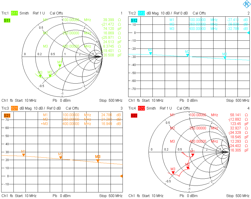 ; they were also exported as a Touchstone file and imported in QucsStudio in order to perform an S-parameter simulation of the second stage together with the matching networks. The project file, which includes the Touchstone file, can be downloaded here; a screenshot of the simulation of the final matching network is here
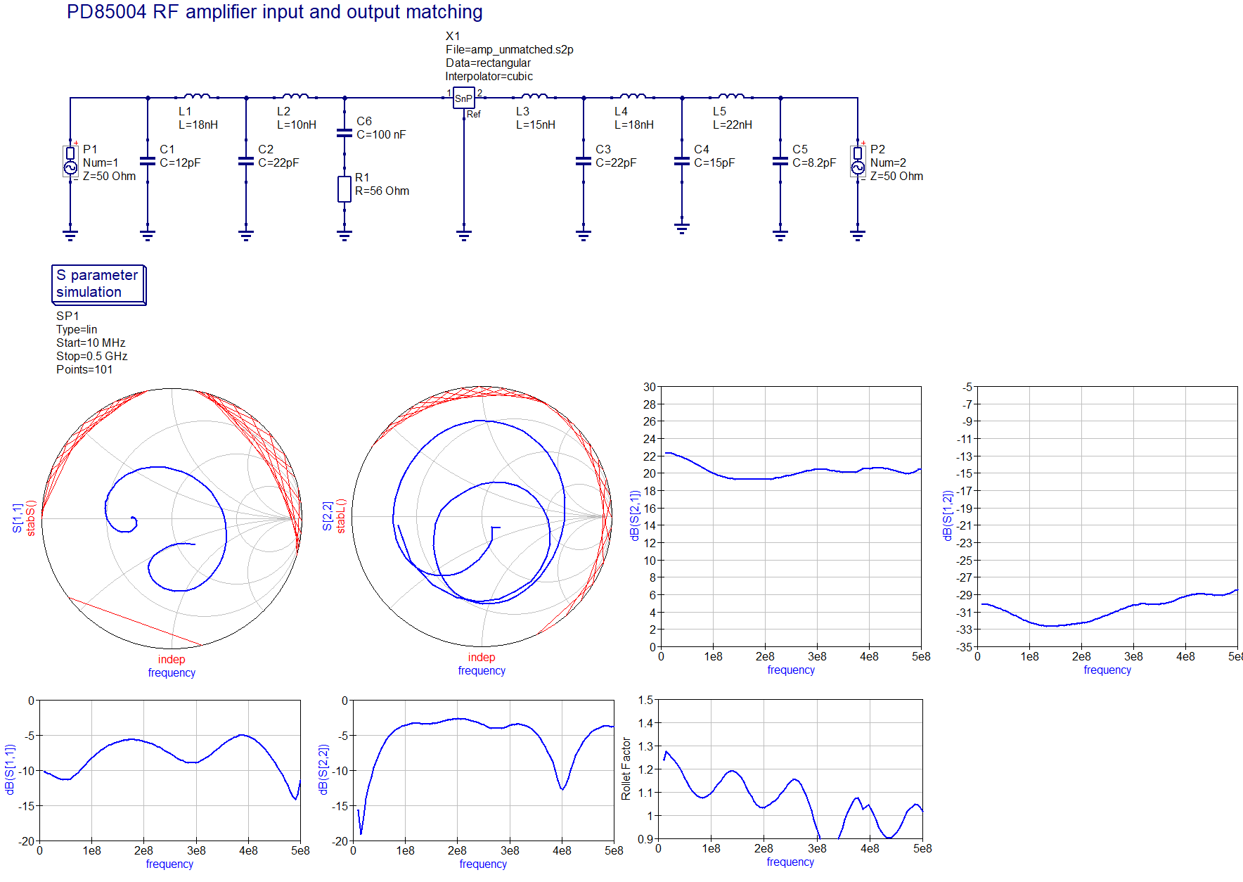 . There are two S-parameter simulations included in the project file, one with the selected E12 component values and another one with the optimizer set up for maximizing S21 with priority while minimizing S11 and S22, and with proper initial values (see the picture
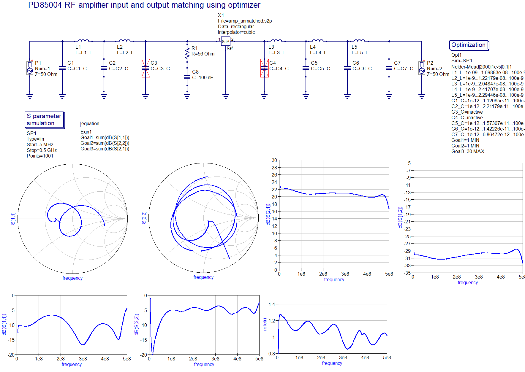 ).
).
One can come up with various solutions of this optimization problem by either optimizing the flatness of various gains (e.g., S21, or transducer gain for given source and load impedances), input and output matching, or output power. The solution that I have adopted tries to maximize S21 flatness (i.e., transducer gain for source and load resistances of 50 ohms) up to 500 MHz at the expense of input and output SWR as well as maximum output power. You can try and experiment yourself with QucsStudio, or come up with another type of matching network. As can be seen, the output SWR of the second stage is not stellar, and it seems not possible to get a return loss better that 5 dB with a purely reactive matching network over a frequency band this broad. There are theoretical limits to matching accuracy and bandwidth for lossless networks (the Bode–Fano theorem), and one could resort to a lossy network in order to achieve a better result. I have not done that since if output matching is critical, a 3 dB attenuator can always be attached to the output for a 6 dB improvement of return loss. Out of curiosity I also tried replacing the inductors by a piece of grounded coplanar waveguide, see here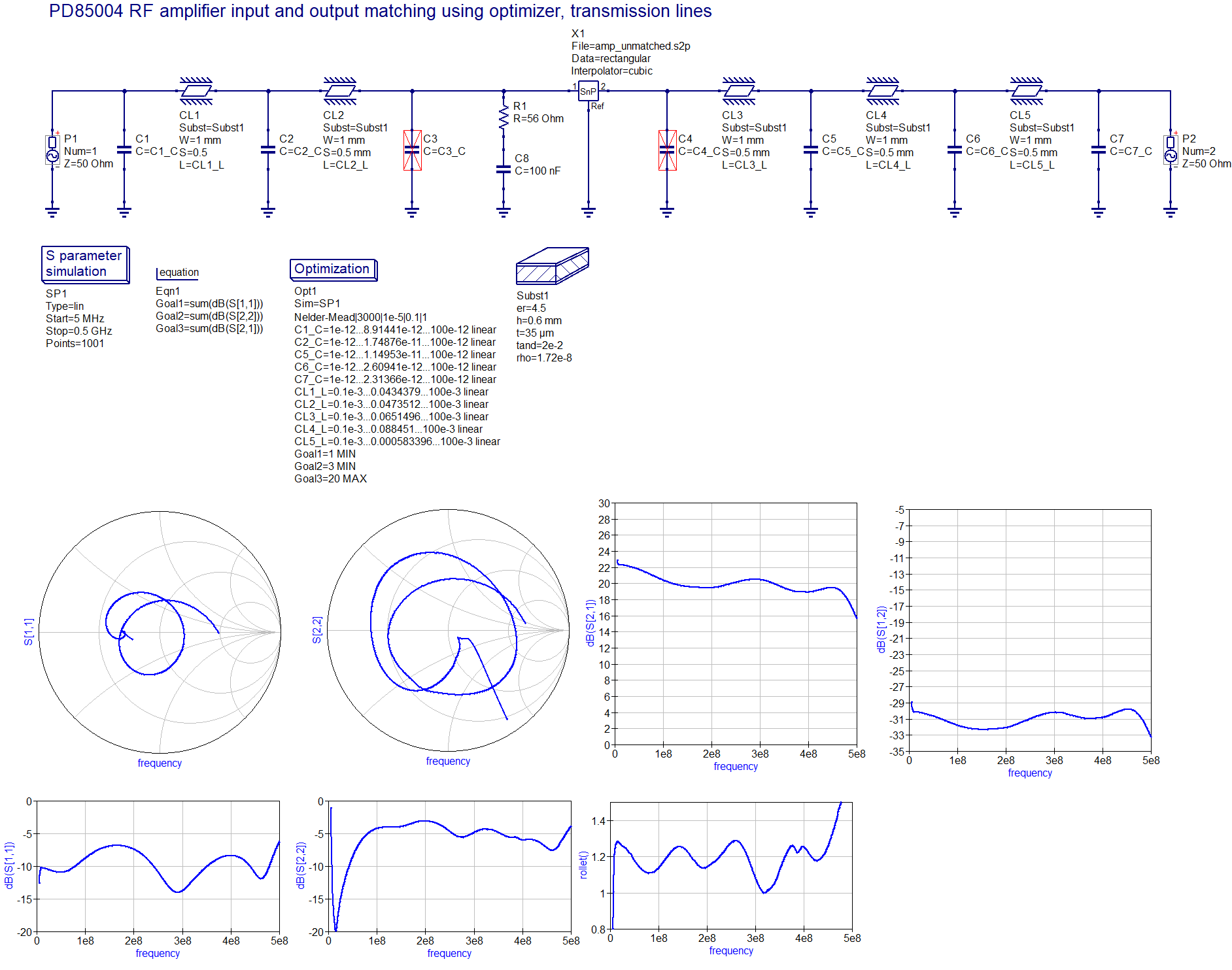 (this is a quick optimizer result for the parameters shown, and can still be tweaked). It does not yield a better return loss, but would consume a lot more board space (notice the lengths of the transmission lines).
Some test results
The most basic measurement to be made are the S-parameters of the amplifier for a small signal input. They were measured for an input of −15 dBm, i.e., at an output power of about 20 dBm. Again, a 20 dB attenuator (calibrated out) at the amplifier output was used.

It is seen that the S21 gain is not as flat as anticipated by the simulation; the flatness is about 3.5 dB except for the small dip at 425 MHz. Among the reasons are the parasitics of the matching networks, which have not been included in the simulation. Moreover, the biasing chokes L1, L2, L3. L4, L5 and L6 have a critical influence, and some variability between different models and manufacturers has been found. In fact, I have changed L1 and L3 for 0805 inductors after the amplifier was assembled since L1 and L3 caused a resonance dip at about 320 MHz. Also the frequency response of the first stage U1 has not been included in the simulation.
Thus, in order to improve flatness, one should redo the simulation with measured S-parameter of the first and the second stage, and include some parasitics of the matching networks. In this way, with some effort and optimization, a flatness of about 1 dB should be achievable.
Moreover, it is seen that the low pass character of the matching networks becomes already noticeable at about 475 MHz, and at 500 MHz the gain has fallen to 25 dB (this is not due to U1 or Q2 running out of steam). The lesson to be learned here is that when recalculating the matching networks for better flatness one should shoot for an upper band limit of, say, 550 MHz to achieve a useful band limit of at least 500 MHz.
Just like gain flatness, output matching is a little worse that predicted by the simulation. The input matching is entirely determined by the HMC311ST89E and its internal matching networks. The input and output SWR resulting from the S-parameters is plotted below.

The reverse isolation of the second stage is already quite appreciable, so it comes as no surprise to find that the amplifier is unconditionally stable over the entire frequency band of 10 MHz to 500 MHz. In fact, its μ1 stability factor, defined as \[\mu_1=\frac{1-\lvert S_{11}\rvert^2}{\lvert S_{22}-\bar S_{11}(S_{11}S_{22}-S_{12}S_{21})\rvert+\lvert S_{12}S_{21}\rvert},\] never falls below 1 and its Rollet factor never below 1.5 in this band.

The next picture shows the harmonic content of the amplifier output at 100 MHz and +25 dBm output level. At this power level the first harmonic is below −15 dBc, the second harmonic is below −30 dBc, and the third below −40 dBc.

Finally, I measured the noise figure of the amplifier with the Y-factor method, using a calibrated noise source. The result shows a noise figure oscillating around 12 dB and peaking at 15 dB. While this is not excellent, it is by no means unusual for commercial amplifiers with comparable data. What remains to be measured are precise values of the first order compression point (estimated to be in excess of 25 dBm) over frequency, the third order intercept point.

These results should also be compared to Claudio Girardi's (IN3OTD), who has experimented with a single stage class A broadband amplifier using the PD85004, and published extensive test results.
Conclusion
Not all the original design goals are fully met by the amplifier. However, by re-measuring the S-parameters of the first and second stage, re-running the simulation and tweaking the matching networks a flatter frequency response up to 500 MHz can be easily achieved. The biasing chokes L1 to L6 have to be carefully selected to avoid resonances within the useful frequency band, or the resonances need to be resistively damped. Ideally, the influence of the particular biasing choke should be included in the measurement data used for the simulation.
Also the output referred 1 dB compression point was found to be somewhat lower than expected, even though the amplifier is not matched for maximum output power. When higher output power is required, the supply voltage and quiescent current of Q2 can be increased. The PD85004 is rated up to 40 V drain-source voltage, 2 A drain current and 6 W total power dissipation, but the cooling concept used here would then have to be improved (the small die cast box would become insufficient as a heat sink). Moreover, R1 should then be decreased to avoid excessive power dissipation, and the associated circuitry be redesigned appropriately.
These experiences show the many difficulties in designing a good broadband amplifier, even at low power levels and over a moderate frequency band. Nevertheless, they can be overcome, and even in its present form the amplifier is a useful laboratory device and ready to be used in practice.