A CW signal generator based on the LMX2582
Recently, PLL synthesizer ICs with integrated wideband VCO and output dividers that are capable of generating signals into the double-digit GHz range have received a lot of attention in the electronics hobbyist community. These chips are easy to set up and offer a performance level and frequency range that was previously only achievable with a board full of complicated RF circuits. Some examples of these chips are the ADF4351 with up to 4.4 GHz output frequency, and the ADF4371 which goes up to 32 GHz, both made by Analog Devices. Competitor Texas Instruments also has a family of integrated PLL synthesizers; examples are the LMX2582 high-performance synthesizer with up to 5.5 GHz output frequency and very low phase noise, or the LMX2595, which goes up to 20 GHz.
To gain some experience with them I tried to design and build CW signal generators based on such chips. The goal was not only to make a proper synthesizer with high frequency resolution, but also with a level-controlled output signal that has low harmonic content. I started with a simple experimental signal generator based the ADF4351. The present page describes a second attempt, this time based on the Texas Instruments LMX2582 high-performance integrated synthesizer. As its predecessor the overall circuit is simplistic and uses a single board design on standard FR4. Nevertheless, it features an accurately leveled output from about −40 dBm to +10 dBm over a frequency range of 20 MHz to 4.2 GHz.
The design is very much derived from its predecessor, with a number of improvements, as well as a simplification since it does not use a DDS to keep the main PLL in integer-N mode in order to avoid integer boundary spurs. This decision was made since it is advantageous to run the LMX2582 with a PFD frequency of greater than 100 MHz for good phase noise performance, so a low noise DDS synthesizer would have been quite costly. Due to the many similarities the following description closely parallels the previous one, with changes in the appropriate places.
Mechanical construction
The signal generator is built on a single four layer board with the dimensions 160×160 mm. The board is lightly populated to facilitate easy manual assembly and soldering. It is housed in a Hammond model 1455 R 1601 extruded aluminium enclosure.


The front and rear panels have been manufactured by Schaeffer AG from Berlin, using their software “Frontplatten-Designer”. The board was designed with KiCad version 5.1.9 and manufactured by JLCPCB with their impedance controlled process using prepreg type 7628. The board layout assumes the the following data:
- Prepreg thickness: 0.2 mm
- Prepreg dielectric constant: 4.60
- Outer layer copper thickness: 35 μm
According to the standard approximation formulas this leads to a 50 Ω microstrip trace width of about 0.349 mm. The top layer of the board is used for RF signals, whereas the bottom layer contains all non-RF control signals; the first inner layer from top is a solid ground plane, the second inner layer is used for power.
Circuit diagram and design data
The schematic of the signal generator consists of seven pages and can be viewed here as a pdf file. The complete design data including KiCad schematic and board files, Gerber files, the firmware source code (written in C), and the front and rear panel artwork, is included in this zip archive. Hopefully, the source code is sufficiently commented to be comprehensible.
Circuit description
The signal generator uses a “headless” design without front panel controls. It is operated as a USB device of class CDC, which establishes a virtual COM port on the host PC. For basic control of the generator a simple terminal program is enough, even though this is not very convenient. It would be better to create some software with a graphical user interface, even though I have not gone to this effort. The USB interface is handled by U22, which is a FT230XS USB to UART bridge by FTDI. It is connected to microcontroller U23, a Microchip (Atmel) ATmega4809-A, which is the brains of the generator and controls all other devices on the board, either via SPI or directly through GPIO lines.
Microcontroller U23 is connected to two general purpose debug LEDs on the main board, which can be useful for firmware development. There are three further LEDs, which indicate lock of the main and reference PLLs, as well an output unleveled condition. Moreover, there are two LEDs which indicate transmit and receive activity on the USB interface. A single front panel status LED is provided; it lights green during normal operation, and red when an error occurs (e.g. a loss of lock of one of the PLLs, the output being unleveled, an argument of a received command being out of range, etc.). Another test facility is a loopback test of the USB data link, which can be enabled by placing a jumper.
Frequency processing starts from the internal reference U6, an accurate 10 MHz TCXO by Connor-Winfield. Then U4, an ultra-low phase noise VCXO running at 100 MHz is phase locked to the reference frequency by means of integer-N PLL chip U5, which is an ADF4002 from Analog Devices. It contains RF and reference frequency dividers, a phase-frequency detector (PFD), a charge pump, and lock detect circuitry. The VCXO is a CVHD-950X-100.00 by Crystek; it features a HCMOS output and a phase noise floor of about −166 dBc/Hz. Resistors R11, R14, and R15 set the appropriate signal levels. The loop bandwidth of the reference PLL is adjusted to about 50 Hz with 50 degrees of phase margin by the three-pole loop filter C33, C34, R13, R17, C35 and C36. In this way the low phase noise of the VCXO is not impaired by the reference, even close to the carrier. Provision is made to connect an external reference frequency. The external reference signal is conditioned by U2, a TLV3501 high-speed comparator by Texas Instruments, and is routed to the reference input of U5 when commanded by microcontroller U23. Resistor R12 and diodes D3 and D4 protect the external reference input.
The phase locked 100 MHz signal from the VCXO is passed on to U8, a LMX2582 wideband synthesizer with integrated VCO by Texas Instruments, after being converted to differential by the 2:1 balun T2. The signal is directly fed to the phase-frequency detector (PFD), all internal reference dividers and doublers are disabled in firmware for best phase noise performance. The VCO of U8, which really is a set of separate VCOs with several bands, operates between 3.55 GHz and 7.1 GHz, and requires a calibration procedure each time the frequency is changed. The firmware of U23 will trigger this calibration procedure upon frequency changes. The maximum output frequency of U8 is 5.5 GHz, although it is only used up to 4.2 GHz in this application in order to limit the number of necessary harmonic filters; the minimum output frequency is 20 MHz. Below output frequencies of 3.55 GHz, several channel dividers included in U8 must be switched into the signal path. There is one divider which can either divide by 2 or 3, and two dividers which can divide by 2, 4, 6 or 8. The dividers can be combined by means of a multiplexer. Microcontroller U23 takes care of the proper setting of the dividers and the multiplexer for a specified output frequency, and keeps the VCO frequency in the allowable range and as small as possible to optimize phase noise.
The main PLL in U8 operates in fractional-N mode unless the VCO frequency happens to be an integer multiple of the PFD frequency of 100 MHz. This is the case for output frequencies of, e.g., 100 MHz, 1 GHz, 2 GHz, etc., at least when no frequency correction or the external reference input is used. Since U8 features a 32 bit resolution in integer-N mode, the minimum frequency step is \begin{align} \Delta f&=f_{\rm pfd}\cdot\text{prescaler}\cdot\frac{1}{\text{denominator}}\cdot\frac{1}{\text{channel divider}}\\ &=100\,{\rm MHz}\cdot2\cdot\frac{1}{2^{32}-1}\cdot1\\ &\approx0.023\,{\rm Hz} \end{align} when no channel division is used, i.e., well below the setting resolution of 1 Hz. The firmware yields a somewhat coarser resolution. This is because the calculation of the fractional-N numerator and denominator values is performed using float instead of double data types. In the version of avr-gcc used for building the firmware, double is only 32 bit wide and is implemented the same way as float. This could be easily improved by using a newer version of avr-gcc, or by implementing the calculation without using double.
The output of U8 is converted from differential to single ended by a wideband 2:1 transmission line type balun T1, which also achieves some gain (3 dB in theory, disregarding its insertion loss). Next down the signal path is the voltage variable attenuator U11, a HMC346AMS8GE by Analog Devices (a former Hittite part), which is controlled by op amp U12. This voltage variable attenuator is part of the automatic level control circuitry.
The voltage variable attenuator is followed by a 9-band harmonic filter bank. The individual low-pass filters are switched by U13 and U14, two HMC321ALP4E GaAs SP8T RF switches by Analog Devices (formerly a Hittite part). Since there are altogether nine filter bands, the lowest two bands are further multiplexed by two MASW-007221 SPDT GaAs switches U9 and U10 from M/A-COM. All switching is done automatically by microcontroller U23, depending on the current output frequency. The following table lists the corner frequency and frequency range of use for each filter:
| Band | Corner freq. (MHz) | Output range (MHz) |
|---|---|---|
| 1 | 39 | 20 … 36 |
| 2 | 69 | 36 … 65 |
| 3 | 124 | 65 … 117 |
| 4 | 220 | 117 … 211 |
| 5 | 400 | 211 … 380 |
| 6 | 720 | 380 … 685 |
| 7 | 1300 | 685 … 1150 |
| 8 | 2340 | 1150 … 2215 |
| 9 | 4200 | 2215 … 4200 |
The filters of band 1 to 7 are realized as lumped component LC filters. After designing them they have been built on a test board and measured with a network analyzer. The filters of band 8 and 9 are realized as microstrip stepped impedance filters; they have been tested in an EM simulation (using QucsStudio with openEMS) and also been measured with a network analyzer. There is good agreement between the EM simulation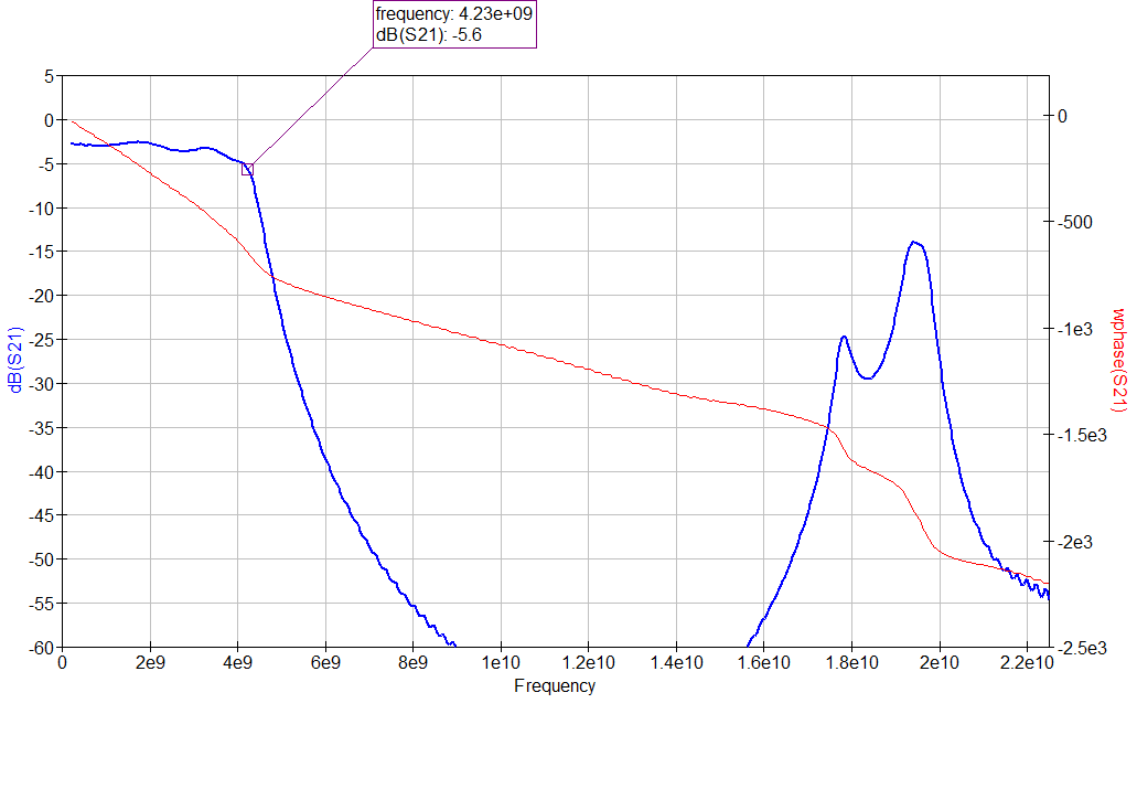 and measurements
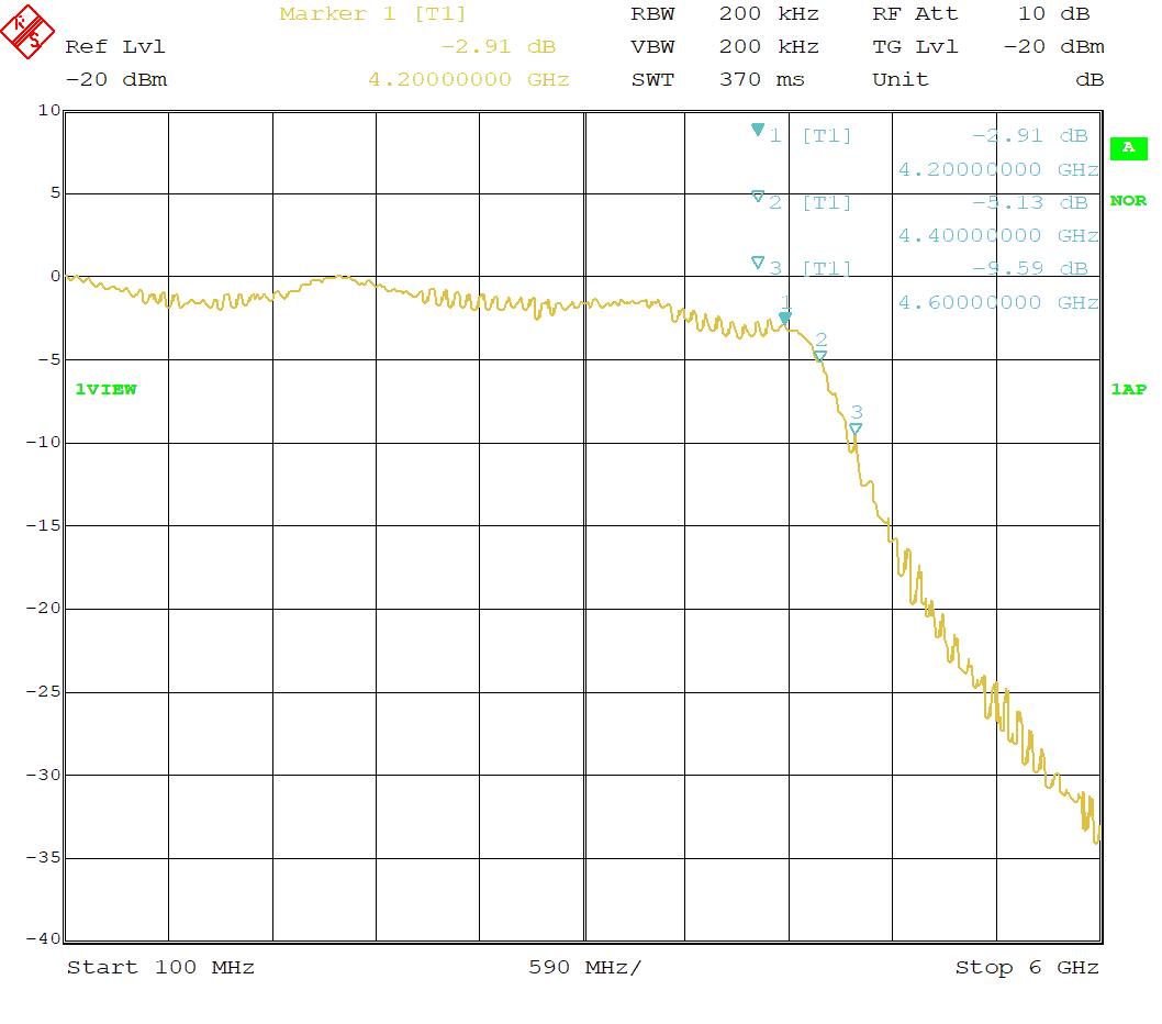 , as shown here for the filter of band 9.
The filter bank is followed by U15, a GVA-81+ InGaP HBT MMIC amplifier from Mini-Circuits. At its output is the resistive signal tap T4, a model RBDC-20-63+ from Mini-Circuits. It taps off a sample of the signal after U15. This is a device with very low insertion loss and a coupling ratio of about 20 dB. The tapped signal is further attenuated by 10 dB by means of MMIC attenuator U18 (HMC656LP2E by Analog Devices) for use by the level detector U19, an AD8319 by Analog Devices. This level detector is part of the automatic level control (ALC) circuitry. After T4, the RF resistor R41 sets the output impedance to 50 Ω.
The ALC control loop is closed within level detector U19, which compares the detected voltage, proportional to the signal level after U15, with the level setting voltage at pin 7 of U16, which is supplied by DAC U25. Between the output of U19 and the voltage controlled attenuator U11 is a low-noise rail-to-rail op amp U20, which shifts the output voltage to the range from −5 V to 0 V, and also sets the ALC bandwidth to approximately 10 Hz. Comparators U21 detect if the output signal is unleveled; this condition is monitored by microcontroller U23.
After the signal tap T4 follows the gain equilibrator T3, which is model EQY-10-63+ by Mini-Circuits, and then U16, a GVA-84+ by Mini-Circuits, another InGaP HBT MMIC with about 24 dB of gain and a 1 dB compression point of about 20 dBm. The purpose of the gain equilibrator is to approximately compensate the roll-off of U16 since it is not within the ALC control loop (it does overcompensate a little, so it would be advantageous to choose a different gain equilibrator). The reason for placing the signal tap between amplifiers U15 and U16, and hence having U16 outside the control loop, is that a loss of 6 dB plus the insertion loss of T4 (about 1 dB) is incurred over T4 and R41. Hence there would not be enough headroom left to drive the output to 10 dBm without adding a too large amount of harmonics.
Finally, U16 is followed by the digitally controllable GaAs MMIC step attenuator U17, which is a HMC629ALP4E by Analog Devices (a former Hittite part). This attenuator can be set between 0 dB and 45 dB in steps of 3 dB, and has an insertion loss of a little less than 3 dB. It is used for coarse level setting, and is under automatic control of microcontroller U23. Fine control of the output level is done by U25, a 12-bit DAC, also controlled by U23. Frequency dependent level correction by means of a calibration table stored in the internal EEPROM of U23 is performed automatically by both DAC U25.
The generator is operated from a DC voltage of approximately 3.3 V to 12 V, supplied to a rear panel barrel jack. The power supply consists of buck/boost converter U29, a LTC3119 by Analog Devices (formerly Linear Technology part), which runs at a switching frequency of a little less than 1 MHz and outputs stable 6 V. This voltage is filtered and passed on to two low dropout linear post regulators U27 and U28, which generate clean 5 V and 3.3 V to power noise critical analog circuitry. Another linear regulator, U26, generates 3.3 V for digital circuitry, with less filtering. Noise critical components such as VCXO U4 and the VCO in U6, have their own local low-noise linear regulators U1 and U7, which are LT3042 by Analog Devices (a former Linear Technology part). Another switchmode converter with Ćuk topology, a LT3462 by Analog Devices (also a former Linear Technology part) generates −5 V to bias the voltage variable attenuator U11. This power rail must also be well filtered. The power input is filtered to prevent switching noise from leaking into the power cable.
Power consumption is about 5 W, depending on input voltage (U29 becomes less efficient for input voltages below 5 V). At 5 V the current consumption is around 1 A.
Operation
As was explained above, the signal generator is operated via a USB CDC interface, which establishes a virtual COM port. In the following, the protocol for controlling the generator is briefly described.
All commands consist of three capital letters. There are two kinds of commands: Setting commands, which have a numerical argument, and interrogation commands, which end with a question mark. The signal generator responds to an interrogation command by sending a string. A string consisting of a command and an argument, or a command and a question mark, must be followed by a newline and/or carriage return character to start execution. Arguments are integer only, no decimal point is allowed. A newline and/or carriage return character flushes the receive buffer. Invalid commands are ignored. Arguments outside permissible bounds generate an error.
The serial interface expects data at 56000 baud, with 8 data bits, one stop bit, and even parity. It sends data with the same parameters. The following table lists all commands.
| Command | Description |
|---|---|
| INF? | Get info string (Signal Generator Mk II, Dr. Mario Hellmich, Salzgitter) |
| VER? | Get firmware version |
| ERR? | Get binary error code, zero means “no error”, also clears the last “argument out of range” error |
| FRQ? | Get current output frequency in Hz |
| LVL? | Get current output level in multiples of 0.1 dBm |
| FRQ [frq] | Set output frequency to frq (from 20000000 to 4200000000, in Hz) |
| LVL [lvl] | Set output level to lvl (from −450 to 100, in units of 0.1 dBm) |
| REF? | Get reference status (0: internal, 1: external) |
| REF [sts] | Set reference status (sts=0: internal, sts=1: external) |
| RFQ? | Get reference multiplier |
| RFQ [mul] | Set reference multiplier to mul (from 10 to 255) |
| SVE [mem] | Save current setup to memory mem (from 0 to 9, generator will always start up from state in memory 0, even when USB is not connected) |
| RCL [mem] | Recall setup from memory mem (from 0 to 9) |
| LCR? | Get level correction value for current frequency |
| LCR [cor] | Set level correction value for current frequency to cor (from −5000 to +5000, in multiples of 0.01 dB) |
| FCR? | Get correction value for internal reference in Hz |
| FCR [cor] | Set correction value for internal reference to cor (from −1000 to +1000, in Hz) |
| SCR? | Get slope correction value for level detector, in multiples 0.01 mV/dB |
| SCR [cor] | Set slope correction value for level detector to cor (from −30000 to +30000, in multiples of 0.01 mV/dB) |
Here are some examples: Sending “FRQ 1500000000\r\n” sets the output frequency to 1.5 GHz. Sending “LVL −100\r\n” sets the output level to −10 dBm. Sending “REF 0\r\n” selects the internal reference.
The reference multiplier works as follows. For an external reference signal with frequency $f$, the reference multiplier $m$ must be set such that $f\cdot m=100\,{\rm MHz}$. For example, when a 5 MHz signal is to be used as external reference, send “RFQ 20\r\n”.
The calibration values for the internal reference, the output level, and the detector slope, as well as ten instrument setups (consisting of output frequency and level, internal/external reference, and external reference multiplier) are stored in the internal EEPROM of microcontroller U23. The firmware is parametrized for 42 level calibration points between 20 MHz and 4.2 GHz, i.e., one point every 100 MHz. The correction value that the LCR? or LCR [cor] commands refer to is determined by the current output frequency. For example, if the output frequency is 123.456 MHz, the current correction value is at 100 MHz. To set the level correction value at, for example, 100 MHz, set generator to that frequency, measure output level, and set correction value with “LCR [cor]\r\n”.
Performance
Spectral purity near the carrier
We start by looking at the spectrum in the vicinity of the carrier. The results for carrier frequencies of 100 MHz, 1 GHz, 2 GHz, 3 GHz and 4 GHz, and at an output level of −10 dBm, are shown in the following pictures. All spectra have been measured with 100 Hz resolution bandwidth and 20 Hz video bandwidth, and with the auto peak detector. Notice that the main PLL actually operates in fractional-N mode since a frequency correction value (using the FCR command) is programmed. Hence there are some integer boundary spurs very close to the carrier. When the frequency correction value is set to zero or the external reference input is used, the main PLL would run in integer-N mode at these frequencies.


The same spectra but recorded with the sampling detector and endowed with phase noise markers can be seen here for carrier frequencies of 100 MHz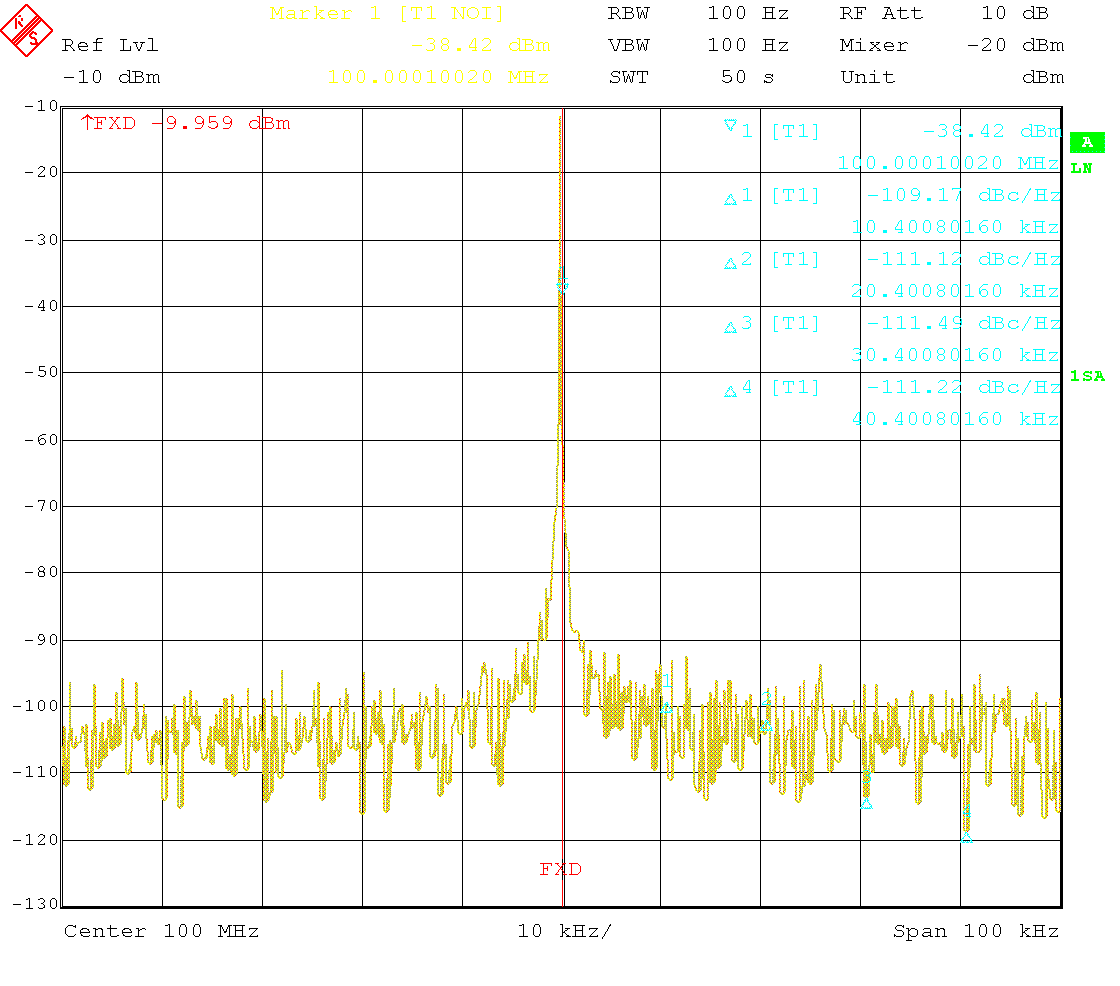 , 1 GHz
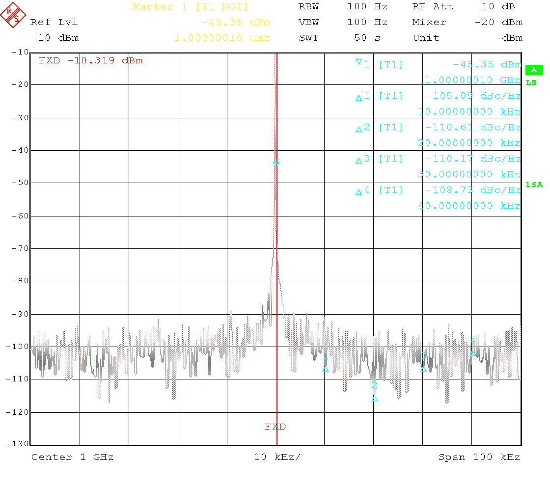 , 2 GHz
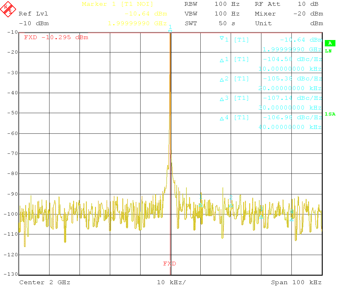 , 3 GHz
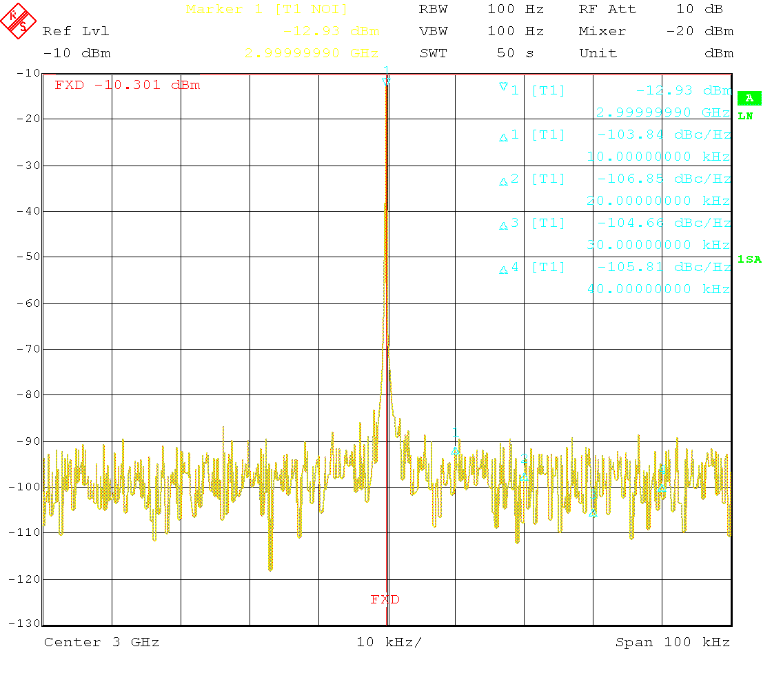 and 4 GHz
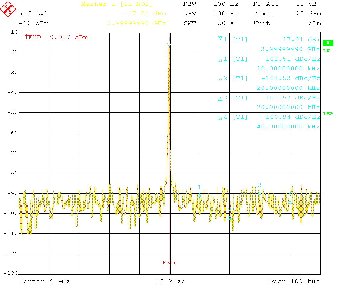 .
.
The following picture compares integer-N and fractional-N operation of the main PLL. The generator is operated from a 10 MHz external reference and set to an output frequency of 1 GHz for integer-N operation, and then to 1.000005 GHz for fractional-N operation. The spectrum shows integer boundary spurs offset at multiples of 5 kHz from the carrier at levels below −50 dBc.

Harmonics and spurs
Next we look at the harmonic and spurious content of the output signal for various carrier frequencies. Also, the spectra in the following pictures indicate the performance of the harmonic filters.


For example, one reads off a harmonic suppression of about 59 dB of the first harmonic for a 1 GHz carrier. Checking some other carrier frequencies shows that a harmonic suppression of at least 30 dB is achieved consistently, and often much better, which is a satisfactory performance. On an oscilloscope, the output signal therefore appears as a perfect sine wave, as can be seen here at 50 MHz and +10 dBm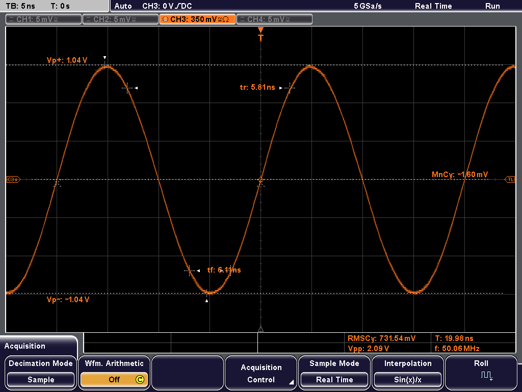 with a scope bandwidth of 500 MHz.
Notice the subharmonic at an output frequency of 4 GHz and at −41 dBc. It appears at output frequencies greater than 3.55 GHz when the LMX2582 is running without a channel divider, and the VCO is routed directly to the RF output. The LMX2582 datasheet talks about a VCO doubler in one place, which could explain the subharmonic, although this may be an error in the datasheet. Unfortunately, there is not much information about the internal structure of the VCO.
There are some low level spurs visible, spaced 100 MHz apart. These are due to the PFD or the reference. They are at levels higher than the specification in the datasheet (less than −93 dBc at a PFD frequency of 20 MHz). The higher spur level are due to the higher PFD frequency of 100 MHz in this application, or possibly to some extent due to a coupling mechanism outside the chip.
Output leveling
Output level accuracy is determined by the level correction values stored in the internal EEPROM of U23. The firmware uses a total of 42 calibration points between 20 MHz and 4.2 GHz, i.e., one point every 100 MHz, with linear interpolation between the points. One could increase this number by changing a parameter in the source code, however, the EEPROM size will set a limit to the number of calibration points (currently EEPROM is used to about 44%).
The level accuracy was measured by sweeping the generator from its minimum to its maximum frequency. This was achieved by controlling it by a GNU Octave script, using the Octave Forge instrument control package. This script is available for download. Running this script and recording the level with a spectrum analyzer set to max hold yields the following result.

The level correction values have been calibrated with a diode power sensor directly connected to the output. The spectrum analyzer, however, was connected by a cable, and had a DC block at its input jack; therefore the level reads a little lower towards higher frequencies.
The traces show a slight wiggle near 795 MHz. This is due to a resonance in the bias tees L30 and L31, and L31 and L33, of MMICs U15 and U16, as has been checked with a network analyzer. This wiggle could be avoided by using different inductors or by adding some damping resistors. Nevertheless, it is not easy to properly bias an amplifier over such a large bandwidth. The spikes seen on the traces are due to switching glitches, which are recorded by the analyzer in max hold mode. They are absent during stationary operation and could be avoided by putting the analyzer as well as the generator under computer control.
The maximum output level obtainable when setting the generator to +10 dBm is shown in the following picture. The dip at 1.15 GHz is also due to the bias networks L30 and L31, and L31 and L33. The generator can maintain a level of +10 dBm until about 3.4 GHz before it slightly drops off and an unleveled condition is indicated. Moreover, the blue trace shows the output when set to a level of −35 dBm. It can be seen that it is off by about 1 or 2 dB at most frequencies. This is because at higher attenuator settings the inaccuracy rises, since the generator was calibrated at an output level of 0 dBm. This inaccuracy could be avoided by calibrating and software correcting the individual attenuator steps.

Settling time
The settling time after frequency or level changes depends on the magnitude of the frequency or level change. The picture below shows an example of a frequency change from 100 MHz to 1 GHz.

The measurement shows a settling time of about 3 ms, mainly due to the narrow bandwidth of the ALC loop. This is not fast, but acceptable for this design. No provisions have been made to achieve a fast locking PLL or low ALC settling times. The LMX2582 offers some facilities to achieve faster locking. By using them, speeding up the ALC loop, and using a faster microcontroller, a much more frequency agile generator could be achieved.
Residual AM and FM
The residual AM and and FM of the carrier was also measured, with the generator locked to an external stable 10 MHz reference, and the main PLL running in integer-N mode. At carrier frequencies of 1 GHz and 4 GHz a residual FM of less than 6 Hz and 10 Hz RMS, respectively, was measured over a bandwidth of 20 kHz. Residual AM was measured to be less than 0.5 % peak over the same bandwidth at both carrier frequencies (the RMS residual AM is much lower). These are satisfactory results.


Conclusion and possible improvements
Compared to its predecessor, which was plagued with some design deficiencies, this generator performs as expected. Moreover, the LMX2582 has a cleaner output signal than the ADF4351, with better phase noise performance (to some extent this is due to the fact that the LMX2582 is operated from a cleaner reference than the ADF4351 in the previous design). There is, however, still a lot of room for improvements, mostly at the expense of a more complex circuit.
One desirable improvement is to drive the main PLL with a DDS synthesizer in order to operate it only in integer-N mode, as was done in the previous design, since this would get rid of the integer boundary spurs. As already mentioned, to keep the good phase noise performance of the LMX2582, this would require a rather sophisticated and costly DDS synthesizer.
Nevertheless, given its simplistic design, the generator performs satisfactorily, and is quite usable in practice.