TRL Calibration
Besides the well known SOLT calibration method (or TOSM in Rohde & Schwarz terms) there are a number of other ways to achieve a full two-port calibration of a vector network analyzer (VNA). One of them is the thru-reflect-line calibration (TRL). As its name implies, TRL uses a through standard, a reflect standard, and one or more transmission lines of appropriate length for the intended frequency range to determine the error terms of the underlying error model, which is somewhat different than the model commonly used for TOSM (but can be mapped to the traditional and more comprehensive error model if some additional quantities, the switch terms, are known).
In TOSM, the match standard is instrumental for calibrating to system impedance. This role is played by the impedance of the line(s) in TRL. A salient feature of TRL is that neither the reflect and the thru, nor the loss of the line(s), need to be accurately known. Since highly precise coaxial airlines or waveguides with very well controlled impedance can be manufactured, TRL can achieve an enormous accuracy.
TRL has the drawback that it only works over a limited frequency band, since the phase shift of the line standard must be within certain limits, and it cannot be sensibly used with very low frequencies (but can be extended to low frequencies by other means). A further issue is that it needs a more complex VNA architecture than TOSM to fully determine the error parameters of the usual 12-term error model. To this end, some measurements must be performed in which both the incident and the scattered wave at a port are measured simultaneously while the other port is configured as a source. Obviously this requires a VNA with four receivers (a so-called dual reflectometer configuration). Therefore true TRL is not available on three receiver VNAs such as the venerable Hewlett-Packard HP 8753, and even less so on transmission-reflection VNAs such as HP 8752, and on virtually all ham radio or hobbyist kit.
Another advantage of TRL is that it lends itself very well to in-fixture calibrations. This is exactly what we shall explore here.
The TRL board
The most simple way to manufacture a test fixture for components like SMD capacitors, inductors, ferrite beads, etc., is to realize it on an ordinary PCB that can be produced with one of the many inexpensive PCB pool services. This allows putting the necessary TRL calibration standards on the board as well. Certainly this does not yield the most accurate test fixture, in particular if the board is ordinary FR4 and one saves on an impedance controlled service, but it has the advantage that the components are tested in their natural environment (i.e., above a ground plane).

The TRL board that I have designed can be seen in the above picture. It contains the following features for calibration, verification, and testing:
- A thru standard for TRL
- A 50 Ω match standard
- A 25 Ω mismatch standard for verification
- An open standard for verification
- A short standard, used as a reflect standard for TRL
- A line of 45 mm length, used as a line standard for TRL
- A series-thru fixture for 0805 components
- A shunt-thru fixture for 0805 components
The board is designed to be usable up to about 2 GHz (it fails to achieve that, see below). The transmission lines and calibration elements on the board are realized as grounded and fenced coplanar waveguides. I have not run a sophisticated 3D EM simulation of the board but instead designed it according to the usual approximation formulas for coplanar waveguides, which should be acceptable at the frequencies involved. The board is designed assuming the following parameters:
- Board thickness: 1.55 mm
- Permittivity: 4.5
- Loss tangent: 0.02
- Copper cladding: 35 µm
- Trace surface: Cu
The SMA launchers are Cinch model 142-0771-831. There are 12 of them, and at a price of about € 7.35 they essentially determine the cost of this amusement. Repeatability of the connectors is vital for precision, but for the limited accuracy requirements here these medium quality ones should be sufficient. The board has been manufactured by JLCPCB from Shenzhen with their standard prototype service. The design files, including Gerber files and Excellon drill files, have been done with KiCad. The schematic for the board is available as a pdf file.
The length of the thru is assumed zero by standard TRL calibration algorithms (unless no offset length is entered into the cal kit definition in the analyzer). This puts the two reference planes at the center of the thru line, thus reference planes are 15.5 mm inwards from each board edge. The reflect (i.e., short), open, match and mismatch standards, correspondingly, are also located 15.5 mm inwards from the board edge, and therefore have zero offset length with respect to the reference planes (notice that this not necessary for the reflect standard in TRL). The line is exactly 45 mm between the reference planes, i.e., its total length is 76 mm. The test fixtures are placed such that the reference planes lie exactly at the outer edges of their SMD pads.
The series-thru and shunt-thru fixtures can both be utilized for impedance measurements, and they are optimal for different impedance ranges. The series-thru configuration is best for measuring higher impedances at higher frequencies (in the kΩ-range and above 100 MHz, say), whereas the shunt-thru configuration is optimal for impedances below 100 mΩ. It is the equivalent of the well-known Kelvin connection used to measure low impedances. There is a third commonly used configuration, which is by connecting the unknown across a single port between the center conductor and ground, and obtaining the impedance from a S11-measurement. This configuration is best in an impedance range from roughly 1 Ω to 10 kΩ and at lower frequencies (up to a couple of 100 MHz). See [1] and [2] for more details on VNA impedance measurements.
When the series-thru or shunt-thru configurations are used, the DUT impedance can be obtained from the corresponding S21-data by way of \[Z=2Z_0\frac{1-S_{21}}{S_{21}}\] for the series-thru configuration, and \[Z=\frac{Z_0}{2}\frac{S_{21}}{1-S_{21}}\] for the shunt-thru configuration. For the single-port configuration the impedance is obtained by \[Z=Z_0\frac{1+S_{11}}{1-S_{11}}.\] In all cases, $Z_0$ is the system impedance.
Some TRL background
In the following I will briefly recall some background information on TRL calibration. I will not, however, give an exhaustive mathematical exposition on how the error terms are determined from measurements of the standards. For this refer to the literature, in particular Dunsmore's book [3] for a leisurely treatment, and the original paper by Engen and Hoer [4] (which is a bit outdated since it assumes a VNA with a dual six-port reflectometer design, which only uses power level measurements to determine the amplitudes and phases of the incident and scattered waves at its two test ports).
The natural error model that goes along with TRL is the 8-term error model. In contrast to the 12-term error model, it requires simultaneous measurements at all four receivers, for which one needs a VNA with dual reflectometer configuration (i.e., with four receiver channels). The error model consists of a virtual transformation network between the reference plane of the measurement and the physical port of the VNA. This virtual network is commonly known as an error box and is described by its four S-parameters. Thus, for two ports there are eight error terms, of which in fact only seven are independent. The mathematics of this setup is most easily described by the transfer matrices $T_{\rm DUT}$, $T_1$ and $T_2$ of the DUT and of the the two error boxes. The transfer matrix that is actually measured by the reflectometers is then found as the product $T_{\rm meas}=T_1T_{\rm DUT}T_2$, from which $T_{\rm DUT}=T_1^{-1}T_{\rm meas}T_2^{-1}$ and finally the corresponding S-matrix $S_{\rm DUT}$ can be obtained.
As in the case of TOSM, a system of equations for the error terms is obtained when the different TRL calibration standards are connected to the VNA ports. This system of equations can be solved for the error terms, and the solutions can be evaluated numerically after the calibration standards have been measured. See, e.g., Dunsmore's book [3] for explicit solutions, and also Pozar's book [5] for an easy derivation under the simplifying assumption that both error boxes are identical, which is, however easily generalized.
The thru standard is usually assumed to be flush, with an S-matrix equal to the unit matrix (i.e., it has length 0 and there is no loss and no reflection). This is appropriate for coaxial flush connections, and in the case of the TRL board presented here it will place the reference planes right in the middle of the coplanar waveguide. If the thru is assumed to have a certain length, i.e., consists of a piece of transmission line, the corresponding calibration scheme is often called line-reflect-line (LRL). The reflect standard only needs to have a nonzero reflection coefficient, which does not need to be known exactly (but its magnitude should be close to 1); it can be obtained as a by-product of the solutions of the TRL calibration equations along with the error terms. However, the reflection coefficient has to be exactly the same for both ports.
The line standard needs to have an impedance equal to the system impedance, but can have losses. Its propagation constant does not need to be known, and can actually be obtained as a by-product from the TRL equations. The line must have a phase shift different from 0° and 180° over the frequency range in which a calibration is to be achieved, because at these frequencies it would not be distinguishable from the thru, and the system of equations for the error terms would be underdetermined. To avoid degradation of accuracy due to noise, the phase shift should not be too close to 0° or 180° (this is checked by common VNA algorithms). A rule of the thumb is to require it to be more than 20° and less than 160°. If a large frequency band is to be covered, it can be split and several lines of different lengths can be used. There is also a variant which simultaneously uses all lines at any frequency with appropriate weighting, known as NIST multiline calibration, see the paper by Marks [6]. This calibration is implemented in the firmware of many modern professional VNAs.
At low frequencies the required line lengths become impractical. Then the line standard can be replaced with a match, which looks like a line with infinite length. Since at low frequencies good match standards are easily available, this is a satisfactory way to extend TRL to low frequencies while maintaining its accuracy at high frequencies. This degenerate case of TRL with a “line of infinite length” in the form of a match is known as thru-reflect-match (TRM) calibration.
In the 8-term error model the two error boxes are independent of the load match of each port, which may change whether the port is configured as a source or a receiver. In fact, it can actually be shown that they are independent of the impedance of the signal source driving the reflectometer. Therefore, in order to transform the 8-term error model into the traditional 12-term model, which explicitly contains separate error terms for source and load match for each direction, additional quantities must be measured. These are the so-called switch terms, which are defined as follows. Let $a_1$, $b_1$ and $a_2$, $b_2$ be the incident and scattered waves at port 1 and 2, respectively. The two switch terms are defined as \[\Gamma_{\rm f}=\frac{a_2}{b_2}\Bigg|_{\text{source at port 1}},\] and \[\Gamma_{\rm r}=\frac{a_1}{b_1}\Bigg|_{\text{source at port 2}}.\] It can be seen that a VNA with four receiver channels is needed to measure these quantities. They are usually measured along with the thru. When the error terms of the 8-term model and the switch terms are known, they can be converted to the standard 12-term error model. (More precisely, the 8-term error model parameters and the switch terms yield 10 error parameters; for the 12-term model, the forward and reverse crosstalk errors also need to be included, which can, however, be neglected in most situations unless there is a non-negligible amount of crosstalk in the test setup.) The explicit transformation equations are easily derived or can be found in the literature (see, e.g., Dunsmore's book [3]).
Board design considerations
As already mentioned, all features on the board are realized with grounded and fenced coplanar waveguides. With the usual approximation formulas for coplanar waveguides, which were used to obtain an impedance of 50 Ω, the design is very straightforward. The launchers are not exactly compatible with the coplanar waveguide structure; the necessary center conductor width is a little bit larger than the line width in the footprint recommended by the manufacturer. See the detail of a screen-shot from the CAD here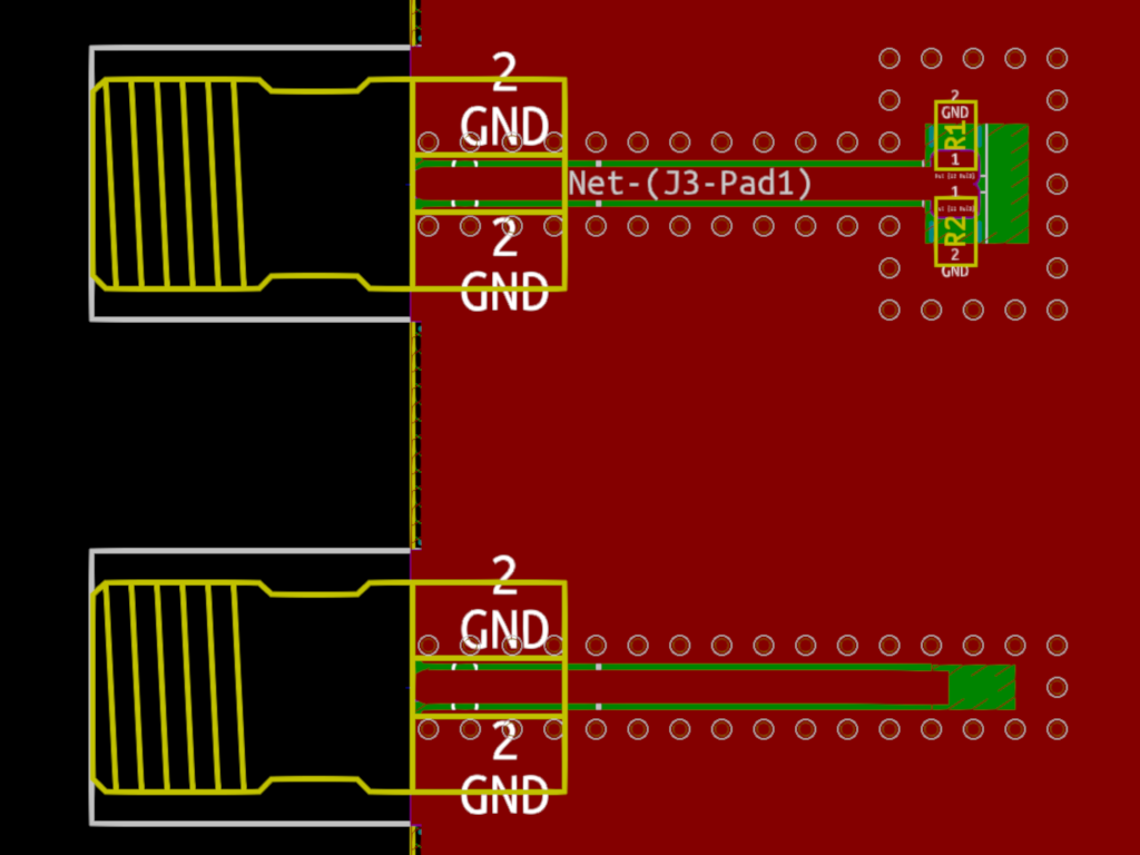 . However, at frequencies below 2 GHz not much error is to be expected as there is no discontinuity in the center conductor width.
The solder mask should not be removed from the component side or from the center conductors of the coplanar waveguides. Even though solder mask may have a poorly defined geometry and permittivity, it will ensure that the trace surfaces are copper when the board is manufactured in a standard pool process. The available surface finishes from most manufacturers are, in general, not very well suited for the present purpose. For example, HAL has a poorly defined surface geometry, and ENIG only yields a very thin gold layer (about 50 to 100 nm) on a much thicker nickel layer (about 5 µm), which is needed as a diffusion barrier. Due to the skin effect a large fraction of the current will flow in the nickel layer, which has a smaller conductivity than copper. Moreover, the nickel layer is deposited in an electroless way with an auto-catalytic reaction using a phosphor compound as reducing agent. Therefore, phosphor will be deposited along with nickel, and depending on the phosphor concentration the nickel layer will have unpredictable and frequency dependent magnetic properties.
Coplanar waveguide impedance
Since in TRL the characteristic impedance of the line is used to calibrate to the reference impedance, it is interesting to determine it by a measurement. We bypass all questions of how to define impedance of a planar circuit, which, strictly speaking, is not well defined as the quotient of voltage and current at a point on the line (even though a grounded coplanar waveguide can be considered to support a TEM mode to a good approximation). Obviously, such a measurement needs an independent calibration which does not use the line as an impedance standard. It is easiest to use a TOSM calibration, which will put the reference planes in the SMA connectors. The drawback is, of course, that then the coplanar waveguide to connector transitions are within the reference planes. Nevertheless, since the line length is large in relation to the transition and no extreme accuracy is required, we shall follow this approach.
There are several ways to measure the characteristic impedance of a transmission line. The first method starts out from the following idea. Suppose that a line of length $\ell$ and with transmission constant $\gamma=\alpha+\mathord{\rm i}\beta$ and impedance $Z$ is shorted at one end. Then, looking into its other end, one sees the impedance \[Z_{\rm in}=Z\cdot\tanh(\gamma\ell).\] Using $\beta=2\pi f/(c_0v_{\rm p})$, where $f$ is the frequency, $c_0$ the speed of light in vacuum, and $v_{\rm p}$ the phase velocity factor, we can measure $Z_{\rm in}$ as a function of frequency and curve fit the above expression to the results in order to obtain the unknowns, among them $Z$. We use the line standard on the board, i.e., the 76 mm coplanar waveguide, and short one of its ends with a SMA short. Then we measure S11 at its opposite end and obtain the impedance from this measurement. The result is plotted below, directly by the analyzer.

After exporting the impedance data from the analyzer, curve fitting to the above expression can be done; the result is plotted here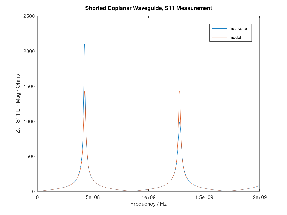 . Curve fitting was done by a GNU Octave script (using the optim package); the script can be downloaded here. Fitting this function is a bit finnicky, and due to the poles the regression algorithm needs good start values. It is seen that the peak height in the model is, unlike the measurement, not frequency dependent. The reason is that the attenuation constant $\alpha$ was assumed to be frequency independent. However, since we are only interested in the coplanar waveguide impedance, this model is adequate. The parameters obtained from the curve fitting are as follows:
- Impedance $Z$: $46.60\;\Omega$
- Attenuation constant $\alpha$: $0.43\;{\rm m^{-1}}$
- Phase velocity factor $v_{\rm p}$: $0.43$
We see that $Z$ deviates from the nominal value of 50 Ω by about −7%. This is within the limits that are to be expected from a non-impedance controlled board manufacturing process. Recall that this result was measured with respect to reference planes in the SMA connectors, and therefore includes errors from the connector to waveguide transition, as well as imprecisions of the short.
There is a more direct way to measure the impedance of a shorted transmission line with a VNA. When a lossless transmission line with impedance $Z$ is shorted at one end, the impedance looking into its other end is \[Z_{\rm in}=\mathord{\rm i}Z\cdot\tan(\beta\ell).\] Thus at the frequencies where $\tan(\beta\ell)=\pm1$, i.e., when $\beta\ell=(2n+1)\pi/4$, $n=0,1,2,\ldots$, we have $Z_{\rm in}=\mathord{\rm i}Z$. These frequencies are easily found by identifying the frequencies $f_{\infty, n}$ of the $n$-th pole, i.e., where $\lvert Z_{\rm in}(f_{\infty, n})\rvert=\infty$. Then at the frequencies \[f_{0,n}=f_{\infty, n}\Bigl(1\pm\frac{1}{4n-2}\Bigr)\] we have $Z_{\rm in}=\mathord{\rm i}Z$, and consequently $\lvert Z_{\rm in}\rvert=\lvert Z\rvert$. This has been demonstrated in the above plot, where the markers M1 and M3 are placed at the first two such frequencies. We obtain 47.787 Ω and 46.041 Ω for the magnitude of the transmission line impedance, in good agreement with the result from the curve fit (notice that the curve fitting method has neglected the frequency dependence of $Z$ and thus gives an average result).
A second and very well known method to measure the impedance $Z$ of a lossy transmission line works as follows. The line is terminated on one end first with an open, and then with a short, and in both cases the impedance at the other end is measured. The impedance looking into the shorted line is $Z_{\rm in}^{\rm s}=Z\cdot\tanh(\gamma\ell)$, as already said above, and $Z_{\rm in}^{\rm o}=Z\cdot\coth(\gamma\ell)$ for the open line. This directly yields \[Z=\sqrt{Z_{\rm in}^{\rm o}Z_{\rm in}^{\rm s}}.\] Hence it is possible to obtain $Z$ as a function of frequency—at least in theory. I have put this method to work, using opens and shorts from a calibration kit. The result can be seen in the following plot.

The result is rather disappointing; the impedance as a function of frequency shows a number of unphysical discontinuities and variations. The reason is the unwieldy progression of $Z_{\rm in}^{\rm o}$ and $Z_{\rm in}^{\rm s}$ with frequency: when one of it has a pole and tends to infinity, the other approaches zero, and vice versa, so that their product remains smooth (in theory the poles of the product are removable). If the open and short used to terminate the transmission line have slightly different offset lengths (an open will always show fringing), the poles and zeros of both functions will not exactly coincide. Moreover, the reflection coefficients of the open and short will be different from ±1. This leads to a progression as shown in the plot, which seriously limits the practicality of this method, even though it is included in may textbooks. One approach to improve this situation could be to fit a mathematical model of the line to the spiky curve obtained from $\sqrt{Z_{\rm in}^{\rm o}Z_{\rm in}^{\rm s}}$.
A third method to measure the impedance of a lossless transmission line, which is somewhat related to the second one, is by terminating one end of the line with an arbitrary but frequency independent impedance $Z_{\rm L}$. Then, looking into the other end, one sees an impedance \[Z_{\rm in }=Z\frac{1+\Gamma\mathord{\rm e}^{-2\mathord{\rm i}\beta\ell}}{1-\Gamma\mathord{\rm e}^{-2\mathord{\rm i}\beta\ell}}=Z\frac{1+\lvert\Gamma\rvert\mathord{\rm e}^{\mathord{\rm i}\arg(\Gamma)}\mathord{\rm e}^{-2\mathord{\rm i}\beta\ell}}{1-\lvert\Gamma\rvert\mathord{\rm e}^{\mathord{\rm i}\arg(\Gamma)}\mathord{\rm e}^{-2\mathord{\rm i}\beta\ell}},\] where \[\Gamma=\frac{Z_{\rm L}-Z}{Z_{\rm L}+Z}.\] With varying frequency or line length, $Z_{\rm in}$ moves on a circle in the Smith chart, and will assume its largest and smallest magnitude when $Z_{\rm in}$ is real. At these frequencies $Z_{\rm in}$ is given by $Z_{\rm max}=Z(1+\lvert\Gamma\rvert)/(1-\lvert\Gamma\rvert)$ and $Z_{\rm min}=Z(1-\lvert\Gamma\rvert)/(1+\lvert\Gamma\rvert)$. This immediately yields \[Z=\sqrt{Z_{\rm max}Z_{\rm min}}.\] This method also has been put to work: the line has been terminated by a SMA termination on one end, and its impedance at the other end has been measured. The result is plotted below. From the formula above and using the first minimum and maximum one finds a line impedance of 47.44 Ω, in reasonably good agreement with the previous result.

There are yet more methods to measure transmission line impedance. One example is the calibration comparison technique which was introduced by Williams, Arz and Grabinski [7]. It employs a two-tier TRL calibration using known impedance standards in the medium one wants to measure (coplanar waveguide on FR4 in this case). First one calibrates by TRL using these standards, and then one performs a second-tier TRL calibration with the unknown line. This will create error boxes at the ends of the unknown line with respect to the first calibration. These characterize the impedance differences, and from them the line impedance can be found. This requires, of course, the availability of known impedance standards, but eliminates the influence of connectors. A method by Marks ans Williams [8] derives the characteristic impedance from a measurement of the propagation constant (which can be obtained as a by-product by solving the TRL calibration equations), the line capacitance, and suitable modeling.
Some applications
It is time to put the board to use. First, a TRL calibration using the TRL standards on the board is performed, where the short is used as reflect standard. Originally the board was intended to be usable up to about 2 GHz, but with that upper frequency limit the analyzer firmware issues a warning since the phase shift of the line exceeds 180°. The reason is some deviations of the board parameters from theory; for the same reason the line impedance deviates a little from 50 Ω, as has been shown above. By an independent measurement I have verified that the line section between both TRL reference planes has 180° phase shift at 1.865 GHz, i.e., at this frequency the line looks looks the tru. For this reason I limit the frequency range to 1.8 GHz for the following measurements.
The first measurement are two 60 Ω ferrite beads in a 0805 SMD package, soldered to the series-thru and shunt-thru test fixtures. The ferrite beads are TDK model MMZ2012R600AT000. Measurement results of the ferrite bead in the series-thru fixture are plotted below.

Let us measure the same setup but with the reference planes in the SMA connectors, as obtained from a UOSM calibration using my cheap SMA calibration kit. The result is plotted below. Observe that the magnitude of S21 does not look much different up to some fractions of a dB, but the phase shift is much larger. As a consequence, the measured impedances are different. In other words, the lines between DUT and reference plane are transforming. This test shows nicely that at the frequencies involved even a few mm of trace matter a lot, and can make a circuit look much different impedance-wise.

Now let's take the same measurements with the shunt-thru fixture; the results are plotted below. As expected, S21 looks very different, however, the calculated impedances are comparable. There are some noticeable deviations, which may be in part due to variations between the two ferrite beads (even though they were taken from the same tape).

Next let's measure a LC parallel resonant circuit, consisting of a 47 nH inductor of size 0805, type LQW2BAS47NJ00L by Murata, soldered on top of a 0805 capacitor with 220 pF and C0G dielectric. The resonance frequency from the nominal component values of this circuit is 49.49 MHz. A TRL calibration with TRM extension to lower frequencies was performed, using the match standard on the board. The same components were successively soldered to the series-thru and shunt-thru fixture and measured. Again, the S21-curves in series-thru and shunt-thru look different, but the calculated impedances in series-thru and shunt-thru configuration match exactly. In the series-thru case a resonance frequency of 49.96 MHz is measured.


Conclusion
A TRL board with test fixtures is a useful tool to have in the lab for quickly testing various components. A good idea for improvement would be to add more line standards to increase the upper frequency limit of the board by multi-line TRL. However, at larger frequencies FR4 tends to become more uncontrollable. For precise measurements one should preferably use an impedance controlled board manufacturing process.
Bibliography
- Keysight Technologies: Ultra-Low Impedance Measurements Using 2-Port Measurements. Keysight Application Note 5989-5935.
- Keysight Technologies: Performing Impedance Analysis with the E5061B ENA Vector Network Analyzer. Keysight Application Note 5991-0213.
- Dunsmore, J.P.: Handbook of Microwave Component Measurements. Chichester: Wiley (2012).
- Engen, G.F, Hoer, C.A.: "Thru-reflect-line": An improved technique for calibrating the dual six-port automatic network analyzer. IEEE Trans. Microwave Theory Tech. 27, 987–993 (1979).
- Pozar, D.M.: Microwave Engineering. 4th Ed. New York: Wiley (2012).
- Marks, R.B.: A multiline method of network analyzer calibration. IEEE Trans. Microwave Theory Tech. 39, 1205–1215 (1991).
- Williams, D.F., Arz, U., Grabinski, H.: Characteristic-impedance measurement error on lossy substrates. IEEE Microwave Wireless Comp. Lett. 11, 299–301 (2001).
- Marks, R.B., Williams, D.F: Characteristic impedance determination using propagation constant measurement. IEEE Microwave Guided Wave Lett. 1, 141–143 (1991).